
PCB Design Services
Understanding the Complexity of the PCB Design Process
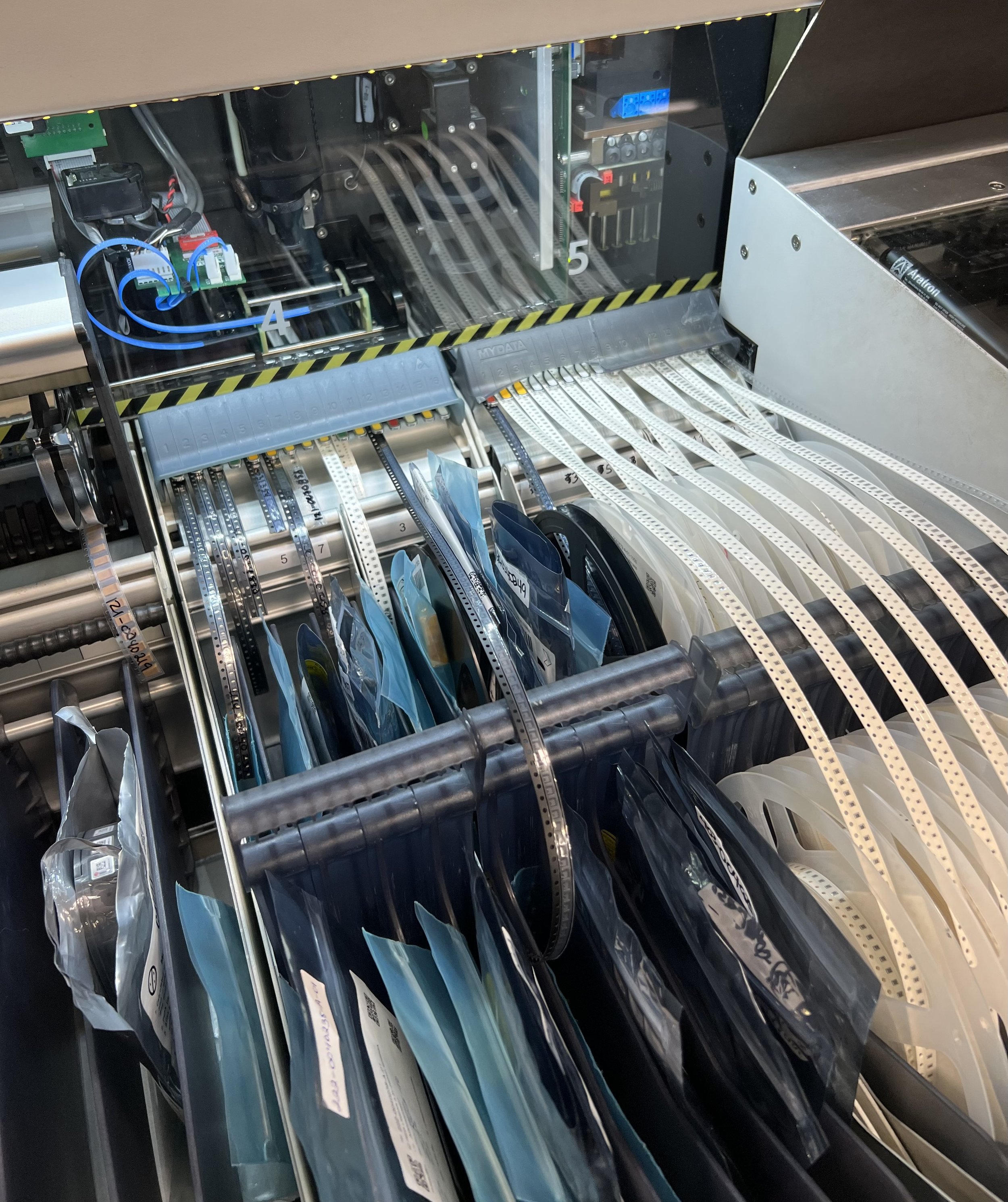
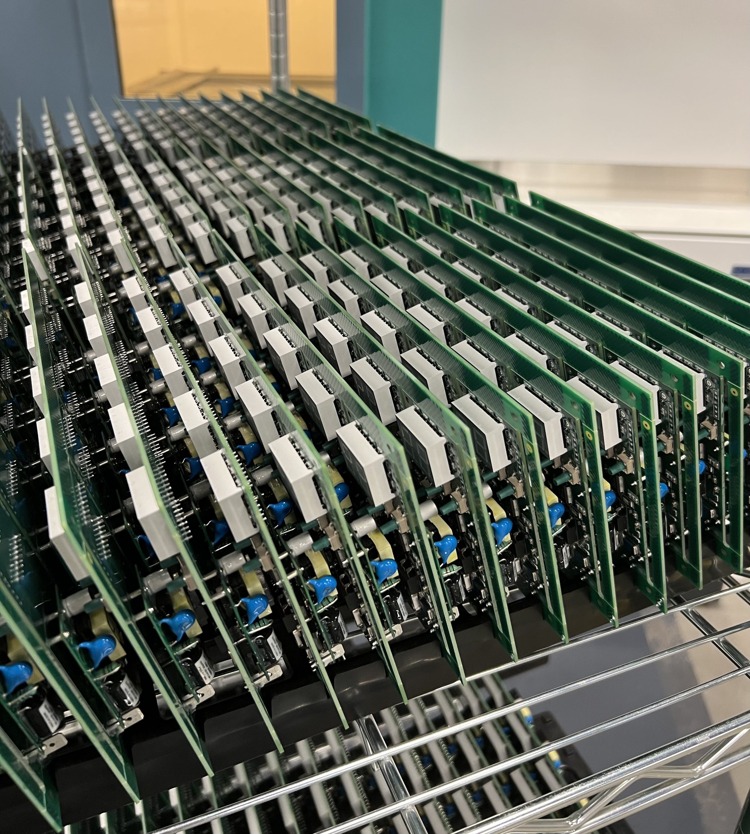
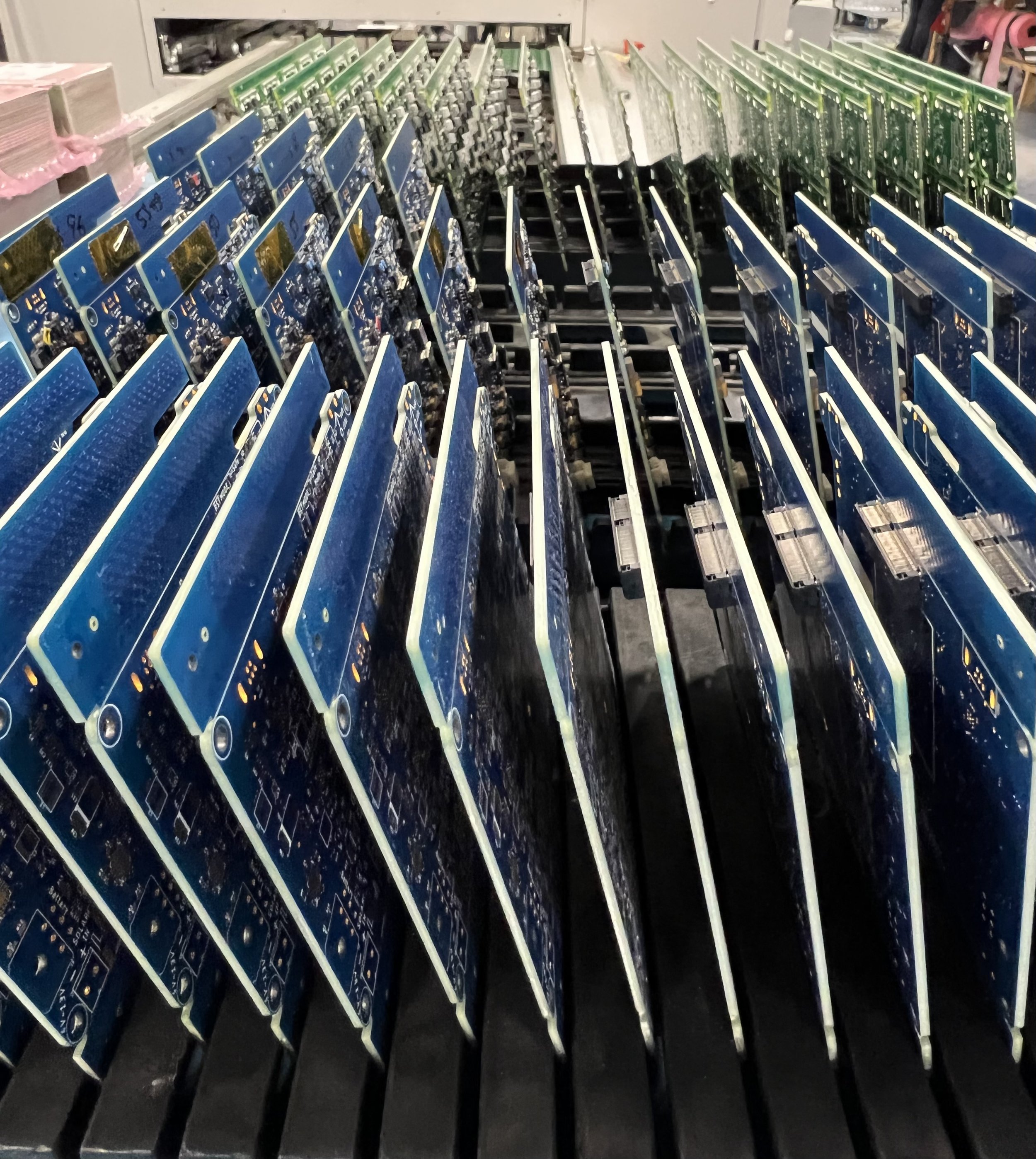
Design: Assembling for Innovation and Functionality
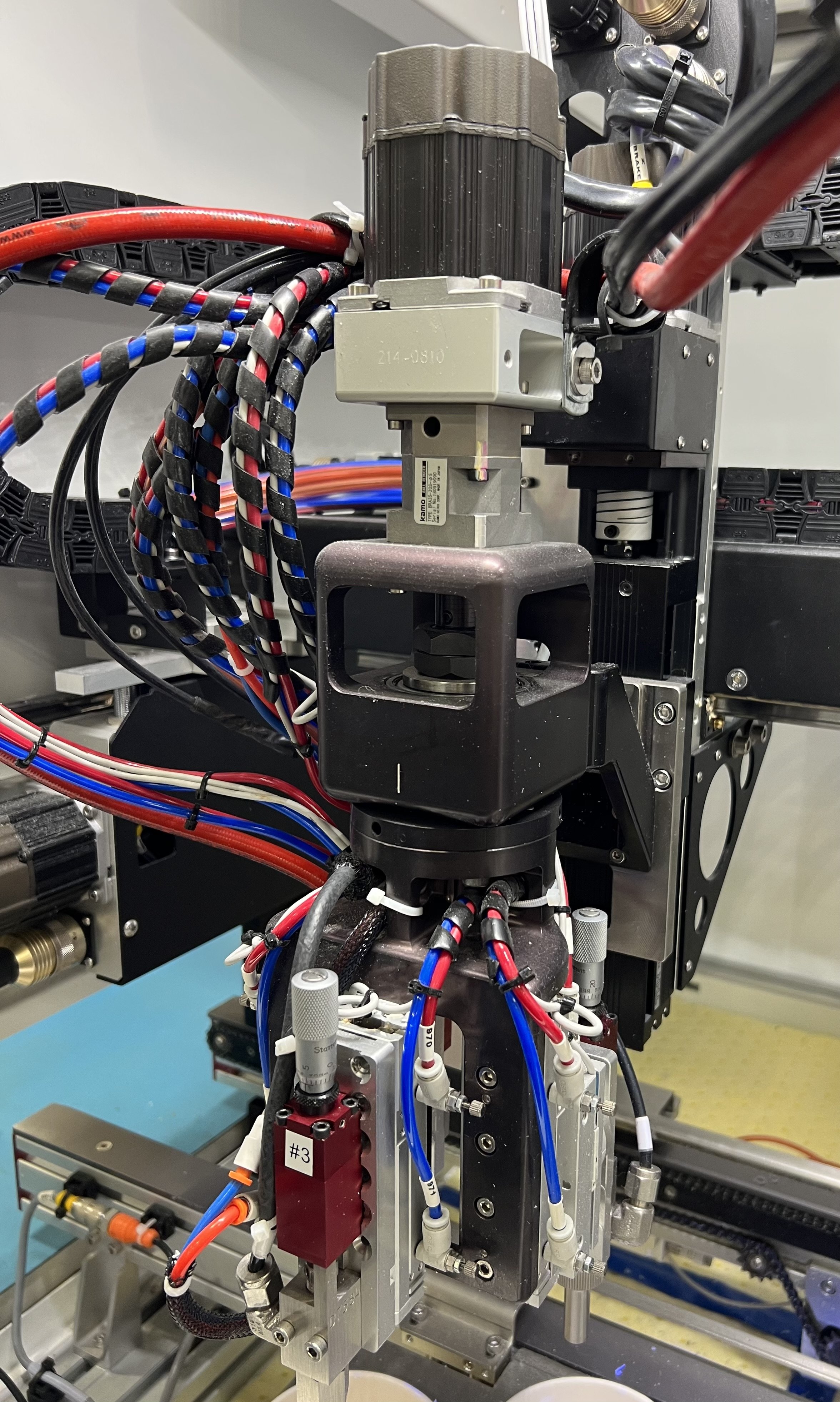
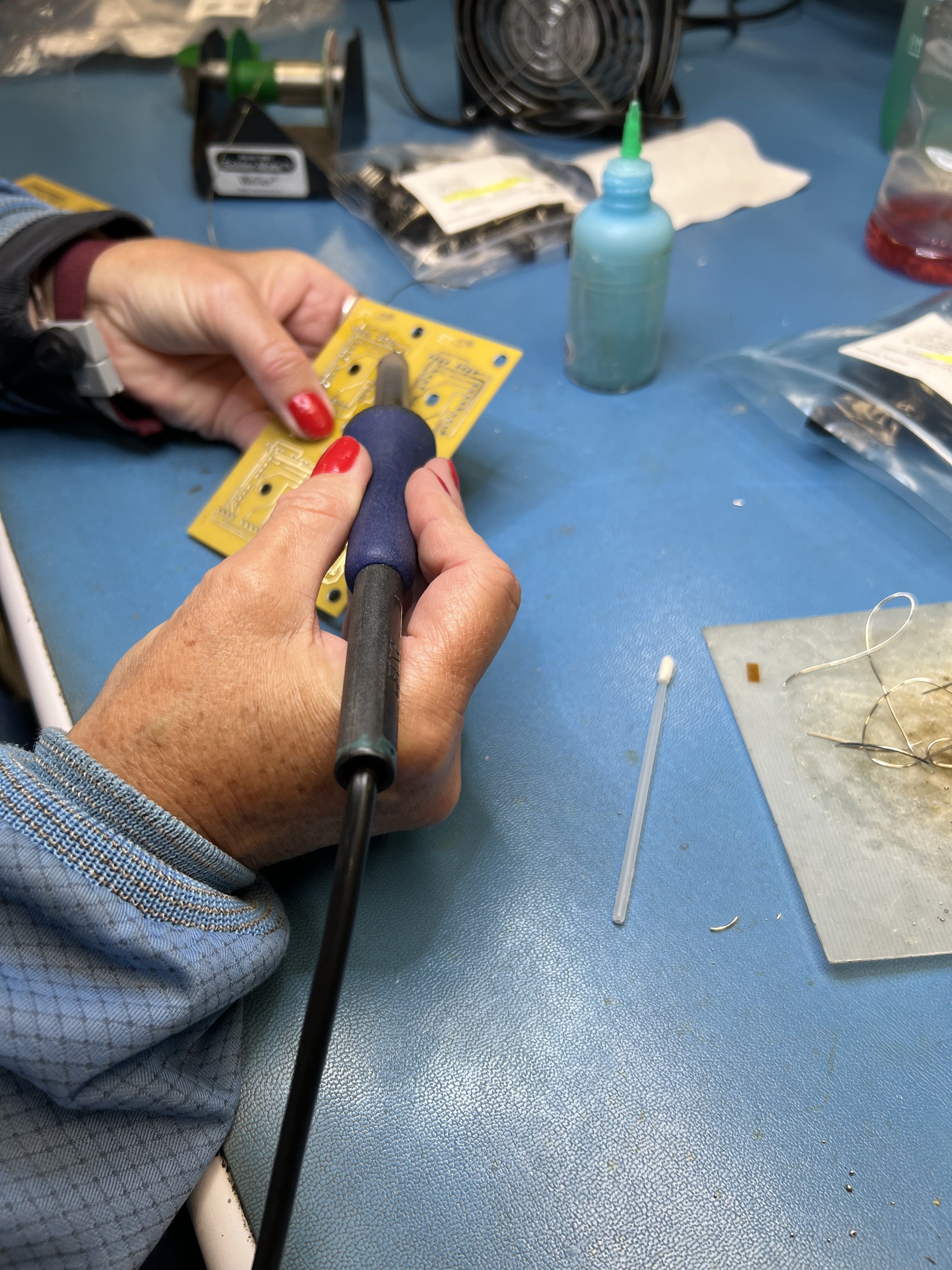
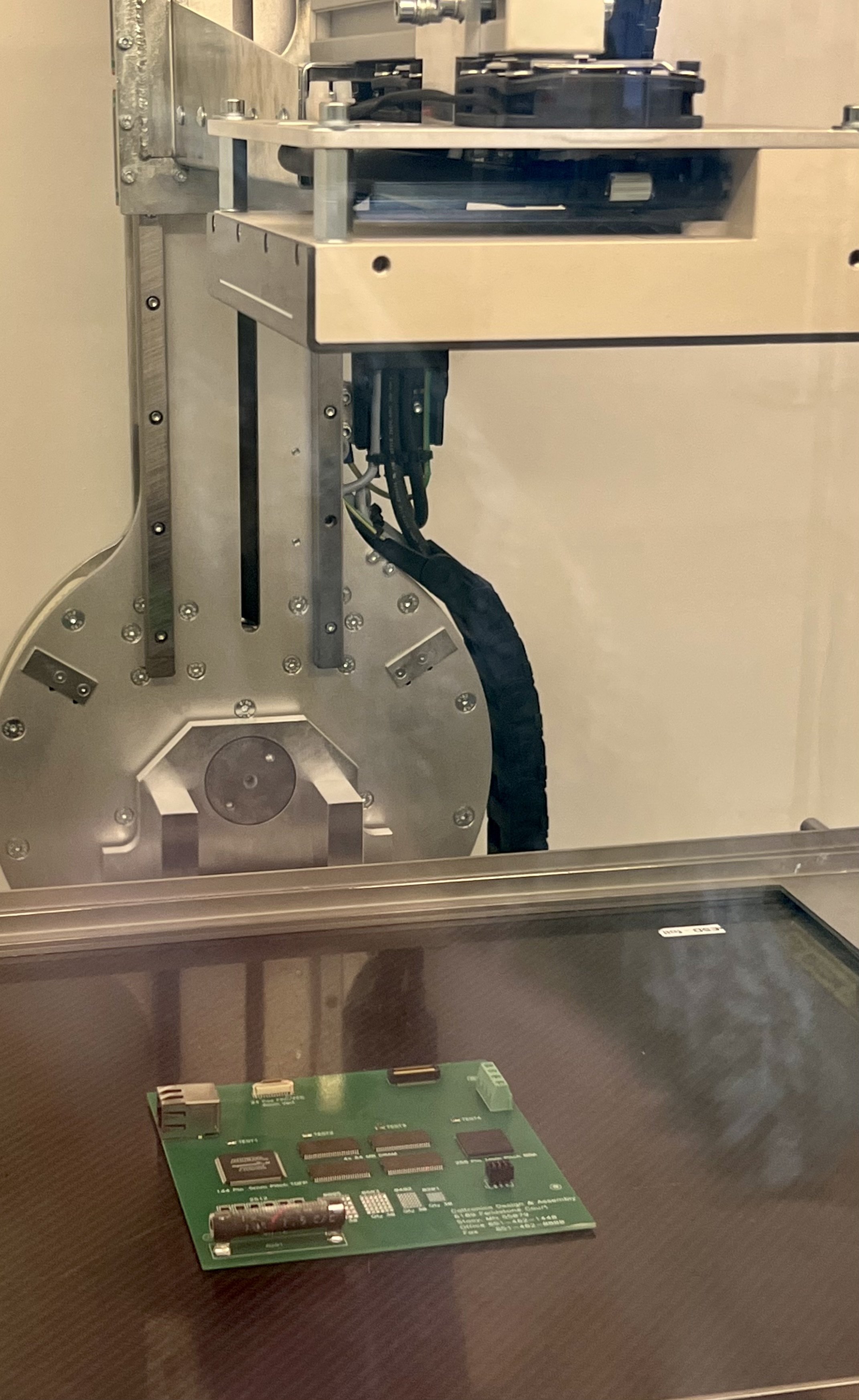
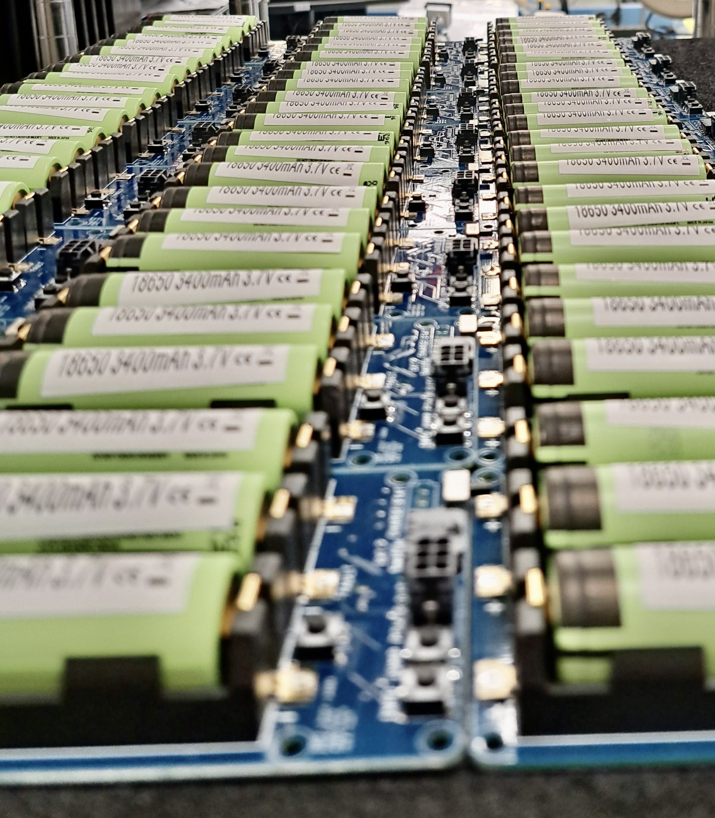
Printed circuit board (PCB) design is an integral process that forms the foundation of your device's functionality. Caltronics’ expert electrical engineers are dedicated to mastering the art of our PCB design services, ensuring your project’s success from concept to realization. Our process is made simple by assembling boards to ensure that any device works for its intended purpose. Sketching the design of the boards, testing, and building an accurate prototype is how we ensure excellence for the products we design.
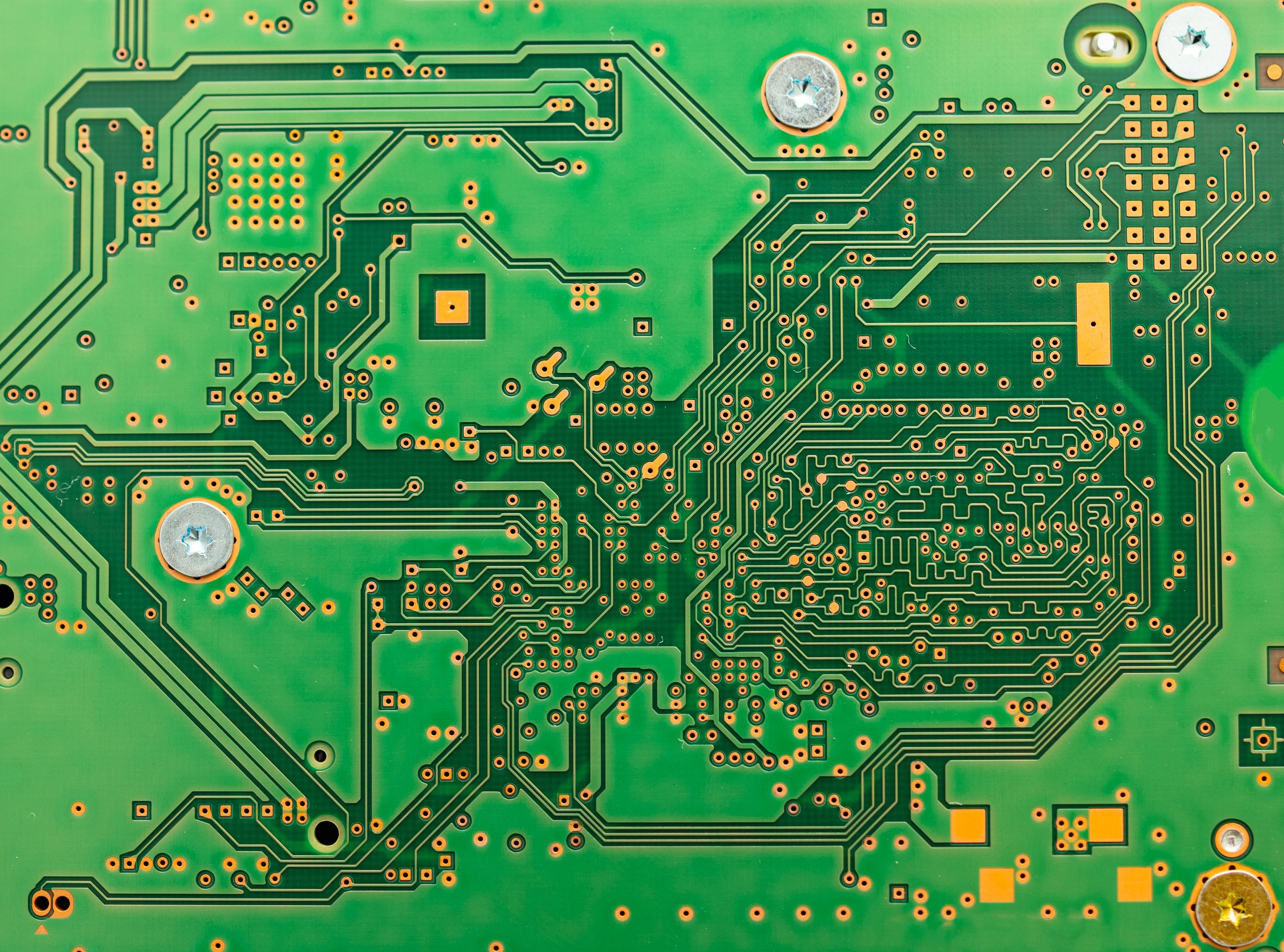
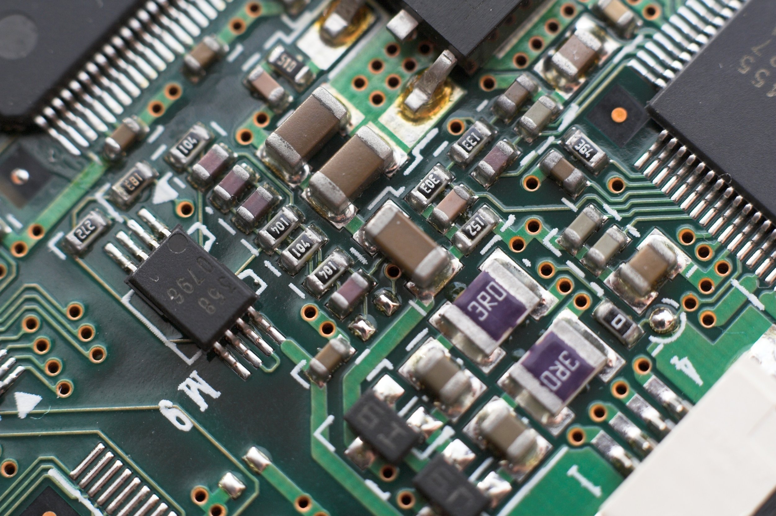
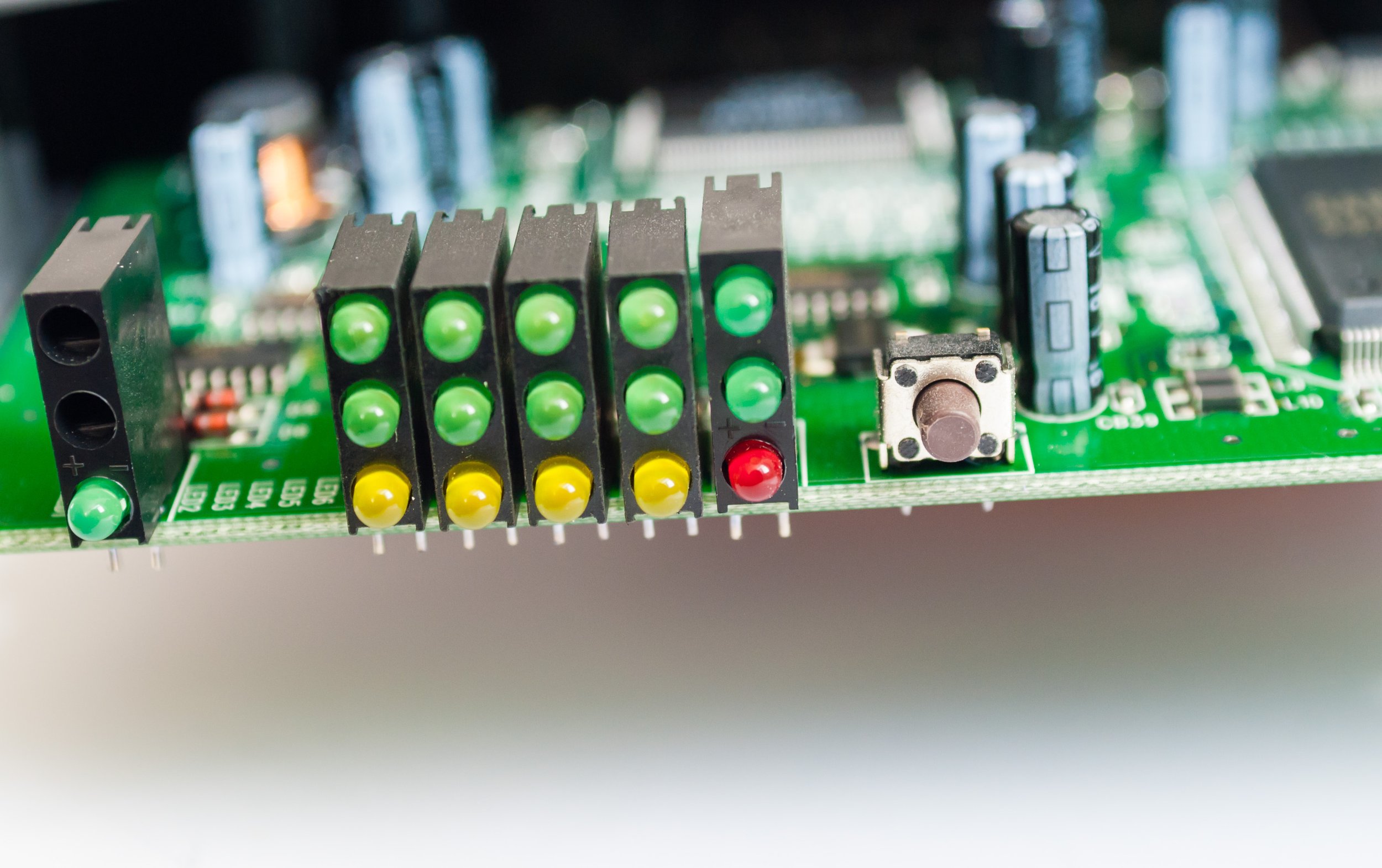
When designing a PCB and the layout design, we consider functionality and manufacturing issues like interference, heat generation, and power management. These determinations ensure you receive PCBs that work in practice and theory. For our customers who desire added functionality in their PCB designs, we also handle embedded microcontroller design, including in-house firmware development with the option to have our staff do the programming.
Choose Caltronics Design & Assembly for expertise in PCB Design
Our team is committed to high-end PCB Design
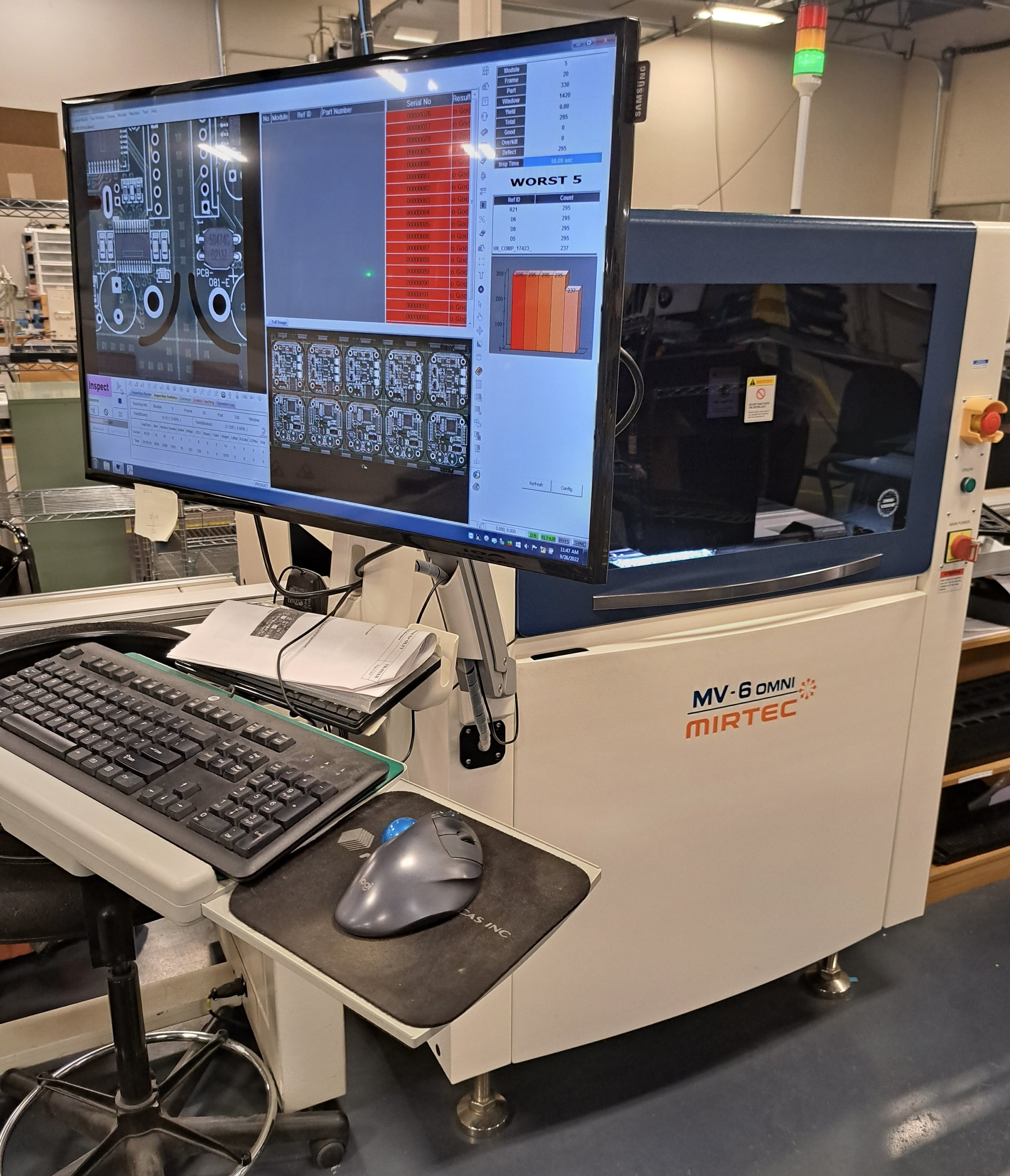
Our team of electrical engineers is an integral part of our in-house assembly process. We are hands-on during the prototyping phase, swiftly identifying and resolving any potential issues or developing new enhancements. We can recognize and pinpoint complications while the prototype is in the assembly process and promptly correct the problem. The electrical engineers who provide the PCB design services will also oversee the manufacturing phase, so the project’s PCB expert is involved in every step. Turn your ideas into reality by using our PCB design services.
We work with a variety of industriess
Between our years of experience and our team of experts, we provide applications for a range of markets to achieve their specific ideas and solutions. Industries we serve include medical devices, aerospace, renewable energy solutions, law enforcement applications, and more. We pride ourselves on innovations that will bring a better tomorrow.
-
![]()
Medical Devices
Create the PCB layout design for fitness, health, or therapy tracking devices, that send data and information to caregivers via Bluetooth.
-
![]()
Renewable Energy
Develop PCB designs that enable devices to monitor and track energy use and provide methods or options for optimizing energy consumption.
-
![]()
Military & Law Enforcement
Help invent training and practice equipment including randomized targets managed through remote control devices.
-
![]()
Aerospace & Defense
Because of the nature of this work, Caltronics is International Traffic in Arms Regulations (ITAR) compliant to protect the secrets of defense-related industries.
-
![]()
Sports and Outdoors
For sports and outdoor equipment, it is critical for the PCB to function and tolerate this environment.


Common PCB Design Services FAQ
What are the materials in a PCB?
What causes a PCB to fail or break?
Printed circuit boards (PCBs) are typically made from copper, resin, and glass. With those being the base elements, there are a lot of smaller elements, such as phenolic cotton paper, epoxy, polyester, and others, that make up the smaller assets of the board's design.
PCB designs are delicate objects, and dropping them from most heights is likely to damage the boards. Damage also comes due to complications from natural elements, exposure to heat, dust, and moisture. Possibly the most critical damage source to protect against is that resulting from Electrostatic Discharges (ESD).
The PCB Design process is broken into four main phases. These steps include:
1. Sketching the initial printed circuit board design
2. Testing the PCB design on a breadboard
3. Creating the PCB layout design
4. Building the PCB design prototype
The early stages require a high level of ideation and fine-tuning the specifics of the concept to develop a device that will operate precisely as you desire. This typically requires more upfront time commitment. Our typical PCB design turnaround is in a few weeks; however, the more complex the product is, the more time it may take to develop the design.
High levels of humidity can lead to corrosion, electrical leakage, insulation breakdown, and distorting signal interference. Significantly impacting the integrity of the board's design.
What is the PCB design process?
How long does the PCB design process take?
How does humidity affect PCB?
A Great Device Starts With an Even Better PCB Design.
Your vision is our driving force for problem-solving the solution.
If you have an idea for a new device, our engineers are here to transform your vision from a concept to a tangible product. Let us know how we can help you with our PCB design services.