3-D AOI: A new dimension in PCB inspection
Move over, 2-D automated optical inspection (AOI). There’s a new kid on the block when it comes to PCB inspection. Introducing 3-D AOI.
With the growing use of surface mount technology (SMT) and chip packages like ball grid arrays (BGAs), solder connection planarity issues come up that call for three-dimensional AOI. 3-D AOI makes it possible for a PCB manufacturer to “see” and measure height differences that can create problems.
PCB inspection is critical
When board layouts were simple, the usual PCB inspection process was manual visual inspection (MVI)—done after soldering and followed by an electrical test at the end of the assembly process. This worked pretty well until SMT came along. SMT’s smaller chip packages allow huge advances in circuit density. With SMT, production rates for consumer products have increased, while already complex boards have become denser and more complex. Demands for faster production and better quality have grown, but MVI can’t keep up. In fact, with MVI as the inspection method, yields drop as volume and complexity go up.
From MVI to AOI to 3-D AOI
Automated optical inspection (AOI) systems are now part of most PCB production lines, usually placed inline after solder reflow so the system can check the quality of solder joints as well as verify that the correct components are in the right places. The AOI systems have many benefits, because they can:
Detect the most common faults in PCB manufacturing
Identify bad boards early in the manufacturing process
Point out failure patterns which may be caused by production problems
Provide fast, accurate result reporting (especially when compared to human inspectors)
Accommodate different PCB designs through quick and easy re-programming
Until recently, AOI systems were 2-D. These systems have performed well except when it comes to measuring height. Even with multi-angle cameras and diverse lighting sources, most 2-D systems can’t reliably and accurately measure height. While Caltronics’ 2-D AOI can measure both BGA height and lifted pins using a laser, only a 3-D AOI system can measure solder fillets with a high level of accuracy.
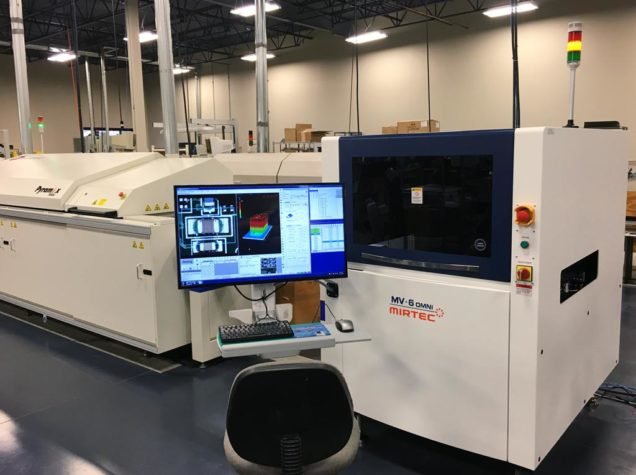
PCB inspection at Caltronics
We offer the latest in 3-D AOI with our award-winning MIRTEC system. Our MV 6 Omni is a high-speed, high-performance system that offers 3-D imaging and analysis, full color processing and 15-megapixel camera technology for accurate inspection of solder quality and small components. Caltronics’ comprehensive inspection program ensures that the PCBs and assemblies we deliver to our clients meet the highest standards of quality. At Caltronics, we use a combination of inline AOI and offline X-ray inspection when needed so our customers get exactly the inspection services and quality PCBs they need.
Learn more
If you’d like to know more about PCB inspection and testing: